Advanced: the RenewableSwitchOver board
Chapter 6 · Introduction to microcontrollers
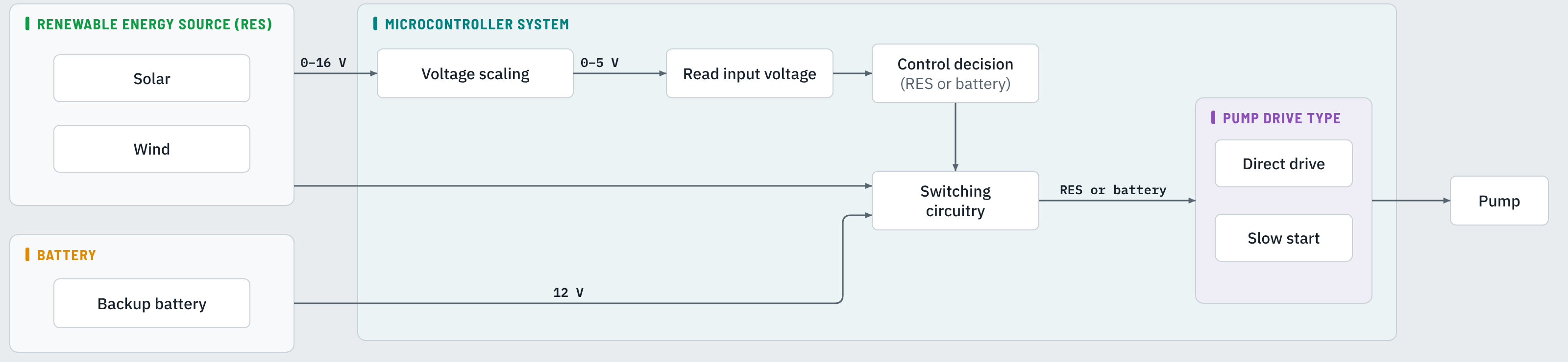
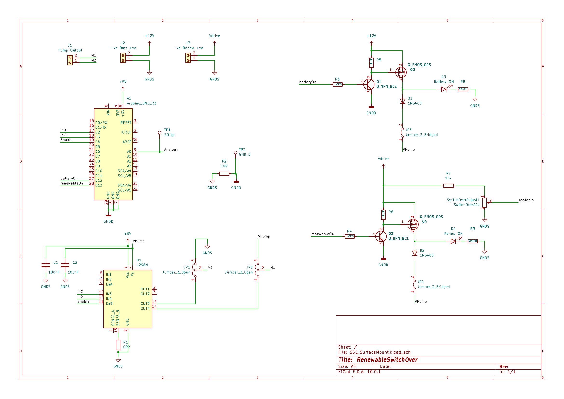
Chapters 1 to 5 built the system from separate parts on a breadboard: a resistor divider, an Arduino, a relay module and an L298N module. The RenewableSwitchOver board puts the same system on one circuit board, with some important differences in how it works. This chapter reads the board’s schematic block by block and matches each part of it to the chapter that introduced the idea.
Learning outcomes
By the end of this chapter you should be able to:
- Read the RenewableSwitchOver schematic and find each block of the project diagram on it
- Set the board’s voltage measurement trimmer safely and measure its divider fraction
- Explain how the board’s high-side P-MOSFET switches, NPN level shifters and diodes select the supply, and compare them with relays
- Explain how the board’s L298N and jumpers provide direct drive or slow start, and why its PWM goes on IN3
- Program the board, using the pin connections from the schematic
1. The schematic
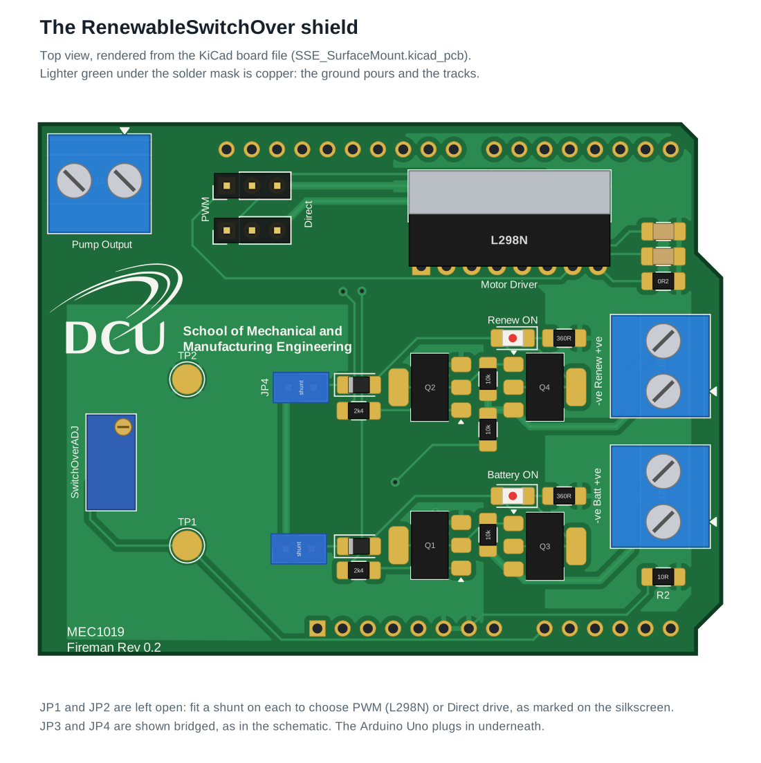
The board itself, rendered from its KiCad layout. Try finding each part from the schematic on it: the silkscreen names some parts (Q1–Q4, TP1, TP2, R2), and the others carry their values (2k4, 10k, 360R, 0R2) or labels (Renew ON, Battery ON, SwitchOverADJ).
A few things help when reading the schematic:
- Net labels. A wire ending in a name such as
batteryOnorVPumpis connected to every other wire with the same name. That is how the Arduino (top left) connects to the switches (right) and the L298N (bottom left) without wires crossing the sheet. - Power symbols.
+12V,+5VandVdriveare supplies;GNDSandGNDDare two separate grounds (Section 5). - Reference designators. Every part has a name: R for resistors, C for capacitors, D for diodes and LEDs, Q for transistors, U for chips, J for connectors, JP for jumpers, TP for test points.
2. The project diagram on the board
| Diagram block | Chapter | On the breadboard | On the board |
|---|---|---|---|
| Renewable energy source (RES) | Project overview | RES wired to the breadboard rails | Screw terminal J3 (Renew): +ve is the net Vdrive |
| Battery | Project overview | Battery wired to the breadboard rails | Screw terminal J2 (Batt): +ve is +12V |
| Voltage scaling | 1 · Voltage measurement | Fixed divider, e.g. 22 kΩ + 10 kΩ | R7 (10 kΩ) and the SwitchOverADJ trimmer; test point TP1 |
| Microcontroller system | 2 · Getting started with the Arduino | Arduino Uno | Arduino Uno A1, plugged into the board |
| Read input voltage, control decision | 3 · Read input voltage | Divider mid-point to A0 | Trimmer wiper (net AnalogIn) to A0 |
| Switching circuitry | 4 · Switching circuitry | Dual relay module, active-LOW | P-MOSFETs Q3, Q4 driven by NPN transistors Q1, Q2, active-HIGH; diodes D1, D2; LEDs D3, D4 |
| Pump drive type | 5 · Pump drive type | Pump on the relays (direct) or on an L298N module (slow start) | U1 (L298N), selected with jumpers JP1, JP2; pump on J1 |
The Arduino’s connections
| Arduino pin | Net | Goes to |
|---|---|---|
| A0 | AnalogIn | Wiper of the SwitchOverADJ trimmer; TP1 |
| D12 | batteryOn | Q1 → Q3: switches the battery in |
| D13 | renewableOn | Q2 → Q4: switches the RES in (and lights the Arduino’s “L” LED) |
| D3 (PWM) | InC | L298N IN3 |
| D2 | InD | L298N IN4 |
| D4 | Enable | L298N EnB |
| 5 V | +5V | L298N logic supply (Vss) |
| GND | GNDD | Driver transistors’ emitters; joined to GNDS through R2 |
Compared with the breadboard version, the supply pins are the other way round (D12 is the battery here, the RES on the relay module), the switches are active-HIGH, and the L298N uses different pins with its PWM on IN3, not on the enable pin.
3. Voltage measurement on the board
The board’s divider is the fixed-resistor-plus-trimmer arrangement from Voltage measurement:
| Part | Connection |
|---|---|
| J3 (Renew) | RES +ve (Vdrive) and RES −ve (GNDS) |
| R7, 10 kΩ | From Vdrive to the top of the trimmer |
| SwitchOverADJ trimmer | Its track from R7 to GNDS; its wiper is the net AnalogIn |
| AnalogIn | Arduino A0, and test point TP1 (SO_tp) |
With a trimmer of total resistance \(R_T\) and \(R_{low}\) below the wiper:
\[V_{A0} = V_{RES}\,\frac{R_{low}}{10\ \text{k}\Omega + R_T}\]
⚠️ Set the trimmer before connecting the Arduino. With a 10 kΩ trimmer turned fully up, a 16 V RES puts 8 V on A0. Check the value printed on your trimmer, then:
- Connect the largest voltage the RES can produce (or a bench supply set to it, e.g. 16 V) to J3.
- Measure from TP1 to ground with a multimeter.
- Adjust the trimmer until TP1 reads just under 5 V (4.8 V gives a margin).
The trimmer is called SwitchOverADJ because it moves the switch-over point: with a fixed threshold in the code, turning it changes the RES voltage at which the threshold is reached (\(V_{RES} = V_{threshold} / k\)).
4. Reading the input on the board
Because the fraction depends on where the trimmer is set, measure it (the same idea as measuring the switch-over reading in Read input voltage):
- Apply a known RES voltage to J3, e.g. 12.0 V from a bench supply, measured with a multimeter.
- Measure the voltage at TP1, e.g. 3.60 V.
- \(k = 3.60 / 12.0 = 0.300\). The code keeps it as a whole number of thousandths, so it needs no
float:const long kRatioPermil = 300;.
Measure again whenever the trimmer is moved.
5. Switching circuitry on the board
The board does the relays’ job with no moving parts: each supply is switched by a P-channel MOSFET, turned on and off by an NPN transistor, and the two switched supplies are joined through diodes. The two switches are identical, so this section follows the battery side (Q1, Q3, D1, D3); the RES side is Q2, Q4, D2, D4 with Vdrive in place of +12V.
High-side P-MOSFET switch: Q3
Q3 sits between the battery’s +12V and the pump supply, on the high side (the positive side). Switching the positive side means the pump’s negative and the supplies’ negatives stay permanently joined to ground, which keeps the shared ground the voltage measurement needs.
A P-channel MOSFET conducts from source to drain when its gate is pulled well below its source:
- Q3’s source is at +12 V. R5 (10 kΩ) pulls the gate up to +12 V too, so the gate–source voltage \(V_{GS} = 0\) and Q3 is off.
- To turn Q3 on, the gate must be pulled down towards 0 V, giving \(V_{GS} \approx -12\) V.
Why the NPN transistor: Q1
The Arduino cannot do that job itself. Its pin only reaches 5 V, so connected straight to the gate it would hold \(V_{GS}\) at about −7 V: Q3 could never turn off, and the 12 V on the gate would reach the Arduino pin. Q1 is a level shifter:
- batteryOn HIGH: current flows through R3 (2.4 kΩ) into Q1’s base: \(I_B \approx (5 - 0.7)/2400 \approx 1.8\) mA, well within the pin’s 20 mA. Q1 saturates and pulls Q3’s gate to almost 0 V. Q3 turns on.
- batteryOn LOW: no base current, Q1 is off, R5 pulls the gate back to +12 V. Q3 turns off.
Q1 only has to sink the current through R5: \((12 - 0.2)/10\,000 \approx 1.2\) mA. Both switches are active-HIGH: digitalWrite(12, HIGH) connects the battery, digitalWrite(13, HIGH) connects the RES.
⚠️ The gate voltage on the RES side follows the RES. With the RES at 16 V, Q4’s \(V_{GS}\) is about −16 V. Check the MOSFET’s maximum \(V_{GS}\) in its datasheet (±20 V is common). At a low RES voltage (a few volts) Q4 is only partly on, but by then the code should have switched to the battery anyway.
The diodes: D1 and D2
The drains of Q3 and Q4 feed the pump supply VPump through D1 and D2 (1N5400: 3 A, 50 V). The diodes form a diode-OR: VPump is fed by whichever switched-in supply is higher, and the other diode is reverse-biased.
They are there for two reasons:
- A MOSFET only blocks in one direction. Every MOSFET has a body diode from drain to source. Without D1, a 16 V RES on VPump would push current back through Q3’s body diode into the 12 V battery, even with Q3 off. D1 blocks it.
- Both supplies can be on at once safely. With relays, both on means the RES and battery are joined directly. With the diodes, current can only flow out of each supply towards the pump, never from one supply into the other.
The price is a forward voltage drop of roughly 0.8–1 V, which the pump never gets, and about \(P \approx 0.9\,\text{V} \times I\) of heat in the diode.
Indicator LEDs, jumpers and test points
- D3 “Battery ON” and D4 “Renew ON” light when their MOSFET is on, each through a 360 Ω resistor (R8, R9), as in the LED circuits of Getting started with the Arduino. At 12 V a red LED draws about \((12 - 2)/360 \approx 28\) mA, and with the RES at 16 V about 39 mA. Check that is within your LEDs’ rating; a larger resistor (e.g. 680 Ω) brings it nearer 15 mA.
- JP3 and JP4 (bridged) are in series with each supply’s diode. Cut or open one to isolate that supply, or to put an ammeter in the path.
- TP1 is A0 (set the trimmer here). TP2 is the Arduino’s ground.
Two grounds: GNDS and GNDD
The board has a supply ground, GNDS (battery −ve, RES −ve, pump, divider, L298N), and a digital ground, GNDD (the Arduino and the driver transistors’ emitters). They are joined at one point through R2 (10 Ω). The large pump current returns through GNDS without passing along the Arduino’s ground wiring, while the two grounds stay at the same potential for the A0 measurement.
Relays or MOSFETs?
| Relay module (Chapter 4) | MOSFET board | |
|---|---|---|
| Switching speed | About 10 ms, with contact bounce | Microseconds, no bounce |
| Wear | Mechanical: contacts wear and arc, especially under load | None |
| Noise | Clicks | Silent |
| Logic | Usually active-LOW | Active-HIGH |
| Voltage lost | Almost none across closed contacts | MOSFET on-resistance plus about 0.9 V across the diode |
| Isolation | Opto-isolators and contacts: no electrical connection to the Arduino | Shares a ground with the Arduino |
| AC or DC | Either | DC only |
| Both supplies on together | Short circuit between the supplies: always break before make | Safe, thanks to D1/D2: can make before break |
Because the diodes make it safe for both supplies to be on for a moment, the board can make before break: switch the new supply on before the old one goes off, so the pump never loses its supply during a switch-over. During reset the Arduino’s pins are inputs, so Q1 and Q2 get no base current and both supplies are off until setup() runs.
6. Pump drive on the board
The jumpers: choosing the drive type
JP1 and JP2 connect the pump terminals (J1: M1, M2) either straight to the supply or to the L298N’s channel B outputs:
| Jumper | Direct drive | Slow start (L298N) |
|---|---|---|
| JP2 → M1 | VPump | OUT4 |
| JP1 → M2 | GND (GNDS) | OUT3 |
Check the positions against the silkscreen on your board. In direct drive, M1 is the positive terminal and the switching code alone runs the pump, exactly as in Pump drive type.
The board’s L298N
| L298N pin | Net | Arduino pin |
|---|---|---|
| IN3 | InC | D3 (PWM) |
| IN4 | InD | D2 |
| EnB | Enable | D4 |
| Vs | VPump | — |
| Vss | +5V | — |
| SENSE_A, SENSE_B | through R1 (0.2 Ω) to GNDS | — |
The L298N module in Chapter 5 takes its PWM on the enable pin. On the board, EnB is on D4, which is not a PWM pin, so the PWM has to go on IN3 (D3, which is). To run the pump the same way round as direct drive, OUT4 must be the positive side. With EnB HIGH and IN4 HIGH:
- IN3 LOW: OUT4 = VPump, OUT3 = GND: the pump is driven.
- IN3 HIGH: both outputs at VPump: the pump’s terminals are joined (brake).
So the drive is the time IN3 spends LOW. To drive the pump at a level from 0 to 255, write the inverse: analogWrite(3, 255 - level).
💡 If the pump’s direction doesn’t matter (or you swap its wires for L298N mode), hold IN4 LOW and write
analogWrite(3, level)directly. Moving Enable to a PWM pin in a future board revision would allow the “PWM on enable” method of Chapter 5.
Other parts around the L298N
- R1 (0.2 Ω) is a current-sense resistor: the voltage across it is \(0.2\,\Omega \times I\), so an oscilloscope across R1 shows the pump current (1 A gives 0.2 V). It is the board’s built-in way to see the inrush current.
- C1 and C2 (100 nF) on +5V and VPump smooth the switching spikes.
7. Code for the board
This combines everything: reading the RES on A0, the switch-over with hysteresis using the MOSFET switches (make before break), and the pump drive through the board’s L298N with the inverted PWM on IN3, with a slow start on both supplies. It has the same structure as Example 5.3 in Pump drive type; the pins, the divider constant and the two hardware functions, setPump() and changeSupply(), differ.
Example 6.1 — the board sketch
/*
 * Example 6.1: RenewableSwitchOver board: supply switch-over with a slow-started pump.
 * Pins from the schematic: A0 = AnalogIn (trimmer wiper),
 *   D13 = renewableOn, D12 = batteryOn (both active-HIGH),
 *   D3 = InC (L298N IN3, PWM), D2 = InD (IN4), D4 = Enable (EnB).
 * Jumpers JP1/JP2 set to the L298N outputs.
 * Whole numbers only: there is no float anywhere in this sketch.
 */

const uint8_t  kSensePin    = A0;
const uint8_t  kResOnPin    = 13;     // renewableOn
const uint8_t  kBatOnPin    = 12;     // batteryOn
const uint8_t  kIn3Pin      = 3;      // InC: a PWM pin
const uint8_t  kIn4Pin      = 2;      // InD
const uint8_t  kEnablePin   = 4;      // Enable (EnB)

// Measured values, kept as whole numbers.
const long     kRatioPermil = 300;    // divider fraction in thousandths, measured at TP1:
                                      //   3.60 V / 12.0 V = 0.300 -> 300
const int      kBatteryMv   = 12000;  // battery voltage in millivolts (measure yours)

// Hysteresis thresholds: RES millivolts, turned into analogRead values by the
// compiler (RES mV x fraction = A0 mV, then x 1023 / 5000).
const int      kToBattery   = 8000L * kRatioPermil / 1000 * 1023 / 5000;  // 8 V -> 491
const int      kToRes       = 9000L * kRatioPermil / 1000 * 1023 / 5000;  // 9 V -> 552

const unsigned long kRampMs   = 2000; // time to reach full drive after a ramp starts
const unsigned long kSampleMs = 100;  // time between RES readings

bool          onBattery    = false;
uint8_t       level        = 0;       // pump drive: 0 (off) to 255 (full)
uint8_t       rampFrom     = 0;       // drive level when the current ramp started
unsigned long rampStartMs  = 0;
unsigned long lastSampleMs = 0;

// The RES voltage in millivolts, from an A0 reading. The sums are done in a
// long, because 1023 x 5000 is far too big for an int.
int resMillivolts(int reading) {
  return (long)reading * 5000 / 1023 * 1000 / kRatioPermil;
}

// Drive the pump at 'lvl' (0 to 255). IN4 is held HIGH, so IN3 LOW drives the
// pump (the same way round as direct drive) and IN3 HIGH doesn't: the drive is
// the time IN3 spends LOW, so write the inverse.
void setPump(uint8_t lvl) {
  level = lvl;
  analogWrite(kIn3Pin, 255 - lvl);
}

// Start a ramp from 'from' up to full drive.
void startRamp(uint8_t from) {
  setPump(from);
  rampFrom    = from;
  rampStartMs = millis();
}

// Move the ramp on. Called on every pass of loop(), so it never blocks.
void updateRamp(unsigned long now) {
  if (level == 255) return;
  unsigned long t = now - rampStartMs;
  if (t >= kRampMs) {
    setPump(255);
  } else {
    setPump(rampFrom + (255UL - rampFrom) * t / kRampMs);
  }
}

// Change supply, on either supply the same way. If the new supply is higher,
// first cut the drive so the pump's average voltage stays about the same, then
// let it ramp back up. A lower supply causes no surge, so needs no ramp.
void changeSupply(bool toBattery, int reading) {
  int resMv = resMillivolts(reading);
  int oldMv = toBattery ? resMv : kBatteryMv;
  int newMv = toBattery ? kBatteryMv : resMv;
  if (newMv > oldMv) {
    startRamp((long)level * oldMv / newMv);
  }
  // Make before break: diodes D1/D2 stop the supplies feeding each other.
  digitalWrite(toBattery ? kBatOnPin : kResOnPin, HIGH);
  digitalWrite(toBattery ? kResOnPin : kBatOnPin, LOW);
  onBattery = toBattery;
}

void setup() {
  pinMode(kResOnPin, OUTPUT);
  pinMode(kBatOnPin, OUTPUT);
  pinMode(kIn3Pin, OUTPUT);
  pinMode(kIn4Pin, OUTPUT);
  pinMode(kEnablePin, OUTPUT);

  digitalWrite(kIn4Pin, HIGH);        // sets the pump's direction
  setPump(0);                         // no drive yet
  digitalWrite(kEnablePin, HIGH);     // L298N channel B on

  onBattery = analogRead(kSensePin) < kToBattery;
  digitalWrite(onBattery ? kBatOnPin : kResOnPin, HIGH);
  startRamp(0);                       // slow start from standstill, on either supply
}

void loop() {
  unsigned long now = millis();

  if (now - lastSampleMs >= kSampleMs) {
    lastSampleMs = now;
    int reading = analogRead(kSensePin);
    if (!onBattery && reading < kToBattery) {
      changeSupply(true, reading);    // RES clearly too low
    } else if (onBattery && reading > kToRes) {
      changeSupply(false, reading);   // RES clearly recovered
    }
  }

  updateRamp(now);
}
Run it: Example 6.1 in the board simulator — the sketch running on a model of the board, with each line highlighted as it runs: change the RES and watch the A0 reading, the supply switching, the ramp and the pump current. Pause and step through one pass of loop() at a time, or tick “What if: no ramp” and reset to see the surge the ramp prevents. · Open full screen ↗
How the code works
The big picture: two jobs at once
The sketch has two jobs, and it must never stop doing either of them:
- Watch the RES and choose the supply: every 100 ms.
- Ramp the pump up smoothly whenever it starts, or its supply steps up to a higher voltage: on every pass of
loop().
A slow start on both supplies. On the RES, the start-up surge would make its voltage sag and could trigger a false switch-over (Pump drive type). On the battery, which doesn’t sag, the surge would instead go through the L298N and the sense resistor R1, which can’t carry it (Why the battery needs a ramp too). So the board ramps the pump on both supplies: the current never jumps far above its running value, whichever supply is switched in. The price is a two-second wait for full flow after a start.
There is no delay() anywhere. Instead, loop() runs many thousands of times a second, and each job checks the time with millis() to decide whether it has anything to do right now. This is the non-blocking pattern from Getting started with the Arduino. A delay(2000) for the ramp would leave the RES unwatched for two seconds, which is exactly when a gust or a cloud could need a switch-over.
The code is split into small functions, each doing one thing:
| Function | Job | Called from |
|---|---|---|
resMillivolts(reading) |
Turn an A0 reading into the RES voltage in millivolts | changeSupply() |
setPump(lvl) |
Set the pump’s drive level on the L298N | startRamp(), updateRamp(), setup() |
startRamp(from) |
Begin a ramp from a given level | setup(), changeSupply() |
updateRamp(now) |
Move the ramp on by the time that has passed | every pass of loop() |
changeSupply(toBattery, reading) |
Switch the MOSFETs, cutting the drive first if the new supply is higher | loop() |
The constants: pins and settings
- Pins are named after the schematic’s nets:
kResOnPinisrenewableOn(D13),kBatOnPinisbatteryOn(D12), and the three L298N pins areInC(D3),InD(D2) andEnable(D4). If a board revision moves a net, only these lines change. kRatioPermilis the divider fraction you measured at TP1 (Section 4), in thousandths: 0.300 is stored askBatteryMvis your battery’s voltage in millivolts. Whole units like these keep every sum in whole numbers.
kToBatteryandkToResare the two hysteresis thresholds, worked out by the compiler asanalogReadvalues: 8 V from the RES puts \(8000 \times 0.300 = 2400\) mV on A0, a reading of \(2400 \times 1023 / 5000 = 491\); 9 V gives 552. Below 491 switch to the battery, above 552 switch back; between them nothing changes. TheLin8000Lmakes the compiler uselongmaths, because \(8000 \times 300 = 2\,400\,000\) does not fit in anint.kRampMsis how long a ramp from 0 to full drive takes;kSampleMsis how often the RES is read.
The variables: what the sketch remembers
| Variable | Remembers | Why it’s needed |
|---|---|---|
onBattery |
Which supply is switched in | The hysteresis test depends on it: the threshold to cross is different on each supply |
level |
The pump’s drive level now, 0 to 255 | changeSupply() scales it when switching to a higher supply, and updateRamp() stops when it reaches 255 |
rampFrom |
The level the current ramp started at | A ramp after a switch-over starts part-way up, not from 0 |
rampStartMs |
When the current ramp started | updateRamp() works the level out from the time since then |
lastSampleMs |
When the RES was last read | So it is read every 100 ms, not on every pass |
They are declared outside any function (global), so they keep their values from one pass of loop() to the next.
No float: readings for decisions, millivolts for sums
The sketch never needs a float:
- The decision compares the raw reading with
kToBatteryandkToRes, as in Read input voltage. No conversion is needed at all. - The drive scaling at a switch-over compares the RES and battery voltages, so
resMillivolts()turns the reading into whole millivolts:
return (long)reading * 5000 / 1023 * 1000 / kRatioPermil;Step by step, for a 12.0 V RES (a reading of about 736):
| Step | Sum | Result |
|---|---|---|
| Reading → mV at A0 | \(736 \times 5000 / 1023\) | 3597 mV |
| A0 mV → RES mV | \(3597 \times 1000 / 300\) | 11 990 mV, about 12.0 V |
(long) makes the whole line use long maths: \(736 \times 5000 = 3\,680\,000\) would overflow an int. Multiply before dividing in each step, or the whole number division would throw the precision away (5000 / 1023 alone is 4).
Leaving out float saves well over 1 KB of program memory, and every sum runs in a few microseconds (Read input voltage).
setPump(): the inverted PWM
analogWrite(kIn3Pin, 255 - lvl);On the board, IN4 is held HIGH and the PWM goes to IN3 (Section 6). The pump is driven only while IN3 is LOW, so the drive is the inverse of the analogWrite value:
level |
analogWrite(3, …) |
IN3 is LOW for | Pump |
|---|---|---|---|
| 0 | 255 | 0 % of the time | Not driven (both outputs at VPump) |
| 64 | 191 | 25 % | Slow |
| 128 | 127 | 50 % | Half drive |
| 255 | 0 | 100 % | Full drive: the whole supply |
setPump() is the only function that touches the L298N’s PWM pin, and it also records level. The rest of the sketch thinks in drive levels, 0 to 255, and never needs to know about the inversion. On the breadboard, with the PWM on ENB, only this one line is different.
startRamp() and updateRamp(): a ramp without blocking
startRamp(from) sets the pump to from and notes the level and the time. It returns at once; the ramp itself happens in updateRamp(), a little at a time:
setPump(rampFrom + (255UL - rampFrom) * t / kRampMs);where t is the time since the ramp started. The level rises in a straight line from rampFrom when \(t = 0\) to 255 when \(t\) reaches kRampMs. For a start from standstill (rampFrom = 0, kRampMs = 2000):
| Time since start | Level | Average voltage on a 12 V supply |
|---|---|---|
| 0 ms | 0 | 0 V |
| 500 ms | 63 | about 3 V |
| 1000 ms | 127 | about 6 V |
| 1500 ms | 191 | about 9 V |
| 2000 ms or more | 255 | 12 V (less the L298N’s drop) |
Three details make it work:
255ULforces the sum intounsigned longmaths. \(255 \times 2000 = 510\,000\) is far too big for anint(maximum 32 767) and would overflow.- Multiply before dividing.
t / kRampMsalone would be 0 until the end of the ramp (whole-number division), so the level would jump straight from 0 to 255. if (level == 255) return;Once the pump is at full drive, there is nothing to do, soupdateRamp()returns straight away on every later pass.
changeSupply(): switching without a surge
Only a step up in supply voltage causes a surge (Pump drive type), so the function first compares the old and new supply, the same way in both directions:
int resMv = resMillivolts(reading);
int oldMv = toBattery ? resMv : kBatteryMv;
int newMv = toBattery ? kBatteryMv : resMv;
if (newMv > oldMv) {
  startRamp((long)level * oldMv / newMv);
}
? : picks one of two values: going to the battery, the old supply is the RES and the new one the battery; going back, the other way round.
- RES → battery with the pump at full drive on a 7.8 V RES (a reading of 478, about 7790 mV): the battery is higher, so the drive is first cut to \(255 \times 7786 / 12000 = 165\). The pump’s average voltage stays at about 7.8 V, so there is no surge through the L298N or R1, and the ramp then takes it up to 12 V. The sum is in
longmaths because \(255 \times 7786\) is too big for anint. - Battery → RES at 9.2 V: the RES is lower, so there is no surge and no ramp. The pump simply slows a little.
- Battery → RES at 16 V: the RES is higher, so the drive is cut to \(255 \times 12000 / 16000 = 191\), about 12 V average, then ramped.
The drive is cut before the switch, so the higher supply never meets the pump at the old drive level. Then the switch itself, make before break:
digitalWrite(toBattery ? kBatOnPin : kResOnPin, HIGH);   // new supply on ...
digitalWrite(toBattery ? kResOnPin : kBatOnPin, LOW);    // ... then old supply off
For a few microseconds both MOSFETs are on. That is safe on this board because diodes D1 and D2 stop either supply pushing current into the other, and it means the pump never loses its supply during a switch-over. With the relay module this order would short the RES to the battery: that is why the Chapter 4 and 5 sketches do it the other way round.
setup(): a safe start
The order of the lines matters:
- Pins become outputs. Until now (during reset) they were inputs, so Q1 and Q2 had no base current and both supplies were off.
- IN4 HIGH, then
setPump(0): the direction is set and the pump is not driven (IN3 held HIGH) before the L298N is enabled. - Enable HIGH: the L298N’s channel B is on, but with no drive yet.
- Choose a supply. If the reading is below
kToBattery(491), start on the battery; otherwise on the RES. startRamp(0): the pump starts with a slow start from standstill, on whichever supply was chosen. Even on the battery, it is never a direct start, so the start-up surge never goes through the L298N and R1.
loop(): watching and ramping
if (now - lastSampleMs >= kSampleMs) {This is true once every 100 ms. Subtracting the times, rather than comparing now with a future time, keeps working when millis() rolls over to 0 after about 49 days.
Inside it, the hysteresis test uses onBattery:
- On the RES, only one thing matters: has the reading dropped below 491 (8 V)? If so, change to the battery.
- On the battery, only: has it recovered above 552 (9 V)? If so, change back.
A RES wobbling between 8 and 9 V therefore causes no switching at all. The reading is passed on to changeSupply(), so the decision and the drive scaling use the same sample. Finally, outside the 100 ms test, updateRamp(now) runs on every pass, so a ramp keeps moving even while the RES is being read. Once a ramp has finished, the drive is 255 and updateRamp() returns at once.
A run-through
| When | What the RES does | What the sketch does |
|---|---|---|
| Power-up | 12 V (reading 736) | setup() picks the RES (736 is not below 491) and starts a ramp from 0 |
| 0–2 s | 12 V | updateRamp() takes the drive from 0 to 255; the RES is read every 100 ms and nothing changes |
| 30 s | Drops to 8.5 V (522) | Not below 491: no change (in the dead band) |
| 31 s | Drops to 7.8 V (478) | Below 491: changeSupply(true, 478), about 7790 mV. The battery is higher, so the drive is cut to 165, the battery switched in, then the RES out; the ramp takes 165 back to 255 by 33 s (a ramp always takes kRampMs) |
| 40 s | Recovers to 8.8 V (540) | On the battery, and not above 552: no change |
| 41 s | Recovers to 9.2 V (564) | Above 552: changeSupply(false, 564), about 9190 mV. That is below the battery’s 12 000 mV, so no ramp: switch the RES in, the battery out; the pump carries on at full drive, a little slower |
What differs from the breadboard sketch
| Breadboard (Chapter 5) | Board | |
|---|---|---|
| Supply pins | D12 = RES, D13 = battery | D12 = battery, D13 = RES |
| Supply logic | Active-LOW relays | Active-HIGH MOSFET switches |
| Switch-over order | Break before make | Make before break |
| PWM pin | ENB on D9 | IN3 on D3 (EnB on D4 held HIGH) |
setPump() |
analogWrite(9, level) |
analogWrite(3, 255 - level) |
| Divider fraction | From the two resistors, kR1 and kR2 |
Measured at TP1, stored in thousandths |
The ramp needs the L298N. To bypass it altogether, move JP1/JP2 to the Direct positions: the pump is then on VPump on both supplies, the PWM has no effect, and only the supply switching matters (plain direct drive, with its full start-up surge, now through the MOSFETs and diodes instead).
Key points
- The board is the same system as Chapters 1–5: every block of the project diagram has a matching group of parts on the schematic.
- Voltage measurement: R7 and the SwitchOverADJ trimmer feed A0. Set it at TP1 so the RES maximum gives just under 5 V, and measure the fraction there.
- Switching: each supply has a high-side P-MOSFET (Q3, Q4) driven through an NPN level shifter (Q1, Q2): D12 HIGH connects the battery, D13 HIGH connects the RES.
- Diodes D1/D2 block the MOSFETs’ body diodes and form a diode-OR, so both supplies can be on together safely (make before break), at the cost of about 0.9 V.
- Pump drive: JP1/JP2 choose direct or L298N drive. EnB (D4) isn’t a PWM pin, so the PWM goes on IN3 (D3), inverted, with IN4 (D2) HIGH.
Knowledge check
Test yourself on this chapter. Answers are checked as you go; calculations with New numbers can be tried again with different values.
On the board, which parts form the voltage scaling block of the project diagram?
R7 (10 kΩ) and the SwitchOverADJ trimmer, with the wiper on A0 and TP1
Q1 and Q3
They switch the battery in (switching circuitry).
D1 and D2
They join the two switched supplies (switching circuitry).
The L298N
That is the pump drive.
Put the steps for setting the board’s SwitchOverADJ trimmer safely in order.
Connect the largest voltage the RES can produce (or a bench supply set to it) to J3
Measure the voltage from TP1 to ground with a multimeter
Adjust the trimmer until TP1 reads just under 5 V
Plug in and power the Arduino
With 12 V applied to J3, a multimeter reads 3.6 V at TP1. What divider fraction \(k\) should go in the code as kRatio?
k = V_TP1 / V_RES = 3.6 / 12 = 0.3
On the RenewableSwitchOver board, Arduino pin is batteryOn and pin is renewableOn. Writing to a pin switches that supply on, because the switches are active-.
Why does each P-MOSFET (Q3, Q4) need an NPN transistor (Q1, Q2) between its gate and the Arduino pin?
The gate must swing between the supply voltage (12–16 V) and about 0 V; a 5 V pin can’t pull it high enough to turn the MOSFET off, and must not see 12 V
The MOSFET gate needs about 1 A to switch
A MOSFET gate draws almost no steady current; the problem is the voltage, not the current.
The NPN transistor makes the switch active-LOW
The board’s switches are active-HIGH.
The NPN transistor limits the pump current
batteryOn drives Q1’s base through R3 = 2.4 kΩ. With the pin at 5 V and 0.7 V across the base–emitter junction, what base current flows?
I_B = (5 − 0.7) / 2.4 kΩ = 1.79 mA, well within the pin’s 20 mA.
What do the diodes D1 and D2 do on the board? Select all that apply.
Stop current flowing back from VPump through a switched-off MOSFET’s body diode into the lower supply
Let VPump be fed by whichever switched-in supply is higher
Make it safe for both supplies to be switched on at the same moment
Raise the pump voltage by about 0.9 V
They drop about 0.9 V; the pump gets slightly less than the supply.
The “Battery ON” LED (forward voltage 2 V) is fed from 12 V through R8 = 360 Ω. What current does it draw?
I = (12 − 2) / 360 = 27.8 mA. Compare it with the LED’s rating (often 20 mA).
The relay code switches the old supply off before the new one on. Why can the board’s code switch the new supply on first?
Diodes D1/D2 stop the two supplies feeding each other, so both on for a moment is safe, and the pump never loses power
MOSFETs switch too fast for it to matter
Speed doesn’t help. With no diodes, two supplies joined even briefly would drive current into each other.
The battery and RES are always at the same voltage
The Arduino can’t switch two pins at once
With EnB HIGH and IN4 HIGH, what happens when IN3 is LOW?
OUT4 is at VPump and OUT3 at ground, so the pump is driven (M1 positive, as in direct drive)
Both outputs are at VPump, so the pump brakes
That’s IN3 HIGH, the same as IN4.
The outputs are disconnected and the pump coasts
That’s EnB LOW.
The pump runs backwards at full speed
On the board, IN4 is held HIGH and the PWM goes on IN3, so the pump is driven while IN3 is LOW. Set the analogWrite value on IN3 so the pump gets 75 % drive (±1).
The drive is the time IN3 spends LOW, so write the inverse, analogWrite(3, 255 - level); 75 % drive is 191, written as 64.
How does the board’s code differ from the breadboard sketch? Select all that apply.
The supply outputs are active-HIGH instead of active-LOW
D12 switches the battery and D13 the RES, the other way round from the relay wiring
The new supply can be switched on before the old one goes off
The PWM is written to IN3 as 255 - level instead of to the enable pin
The RES is read on A1 instead of A0
Both read the RES on A0.